
Odisha Launches India’s First Advanced 3D Chip Packaging Unit Backed by US Firm
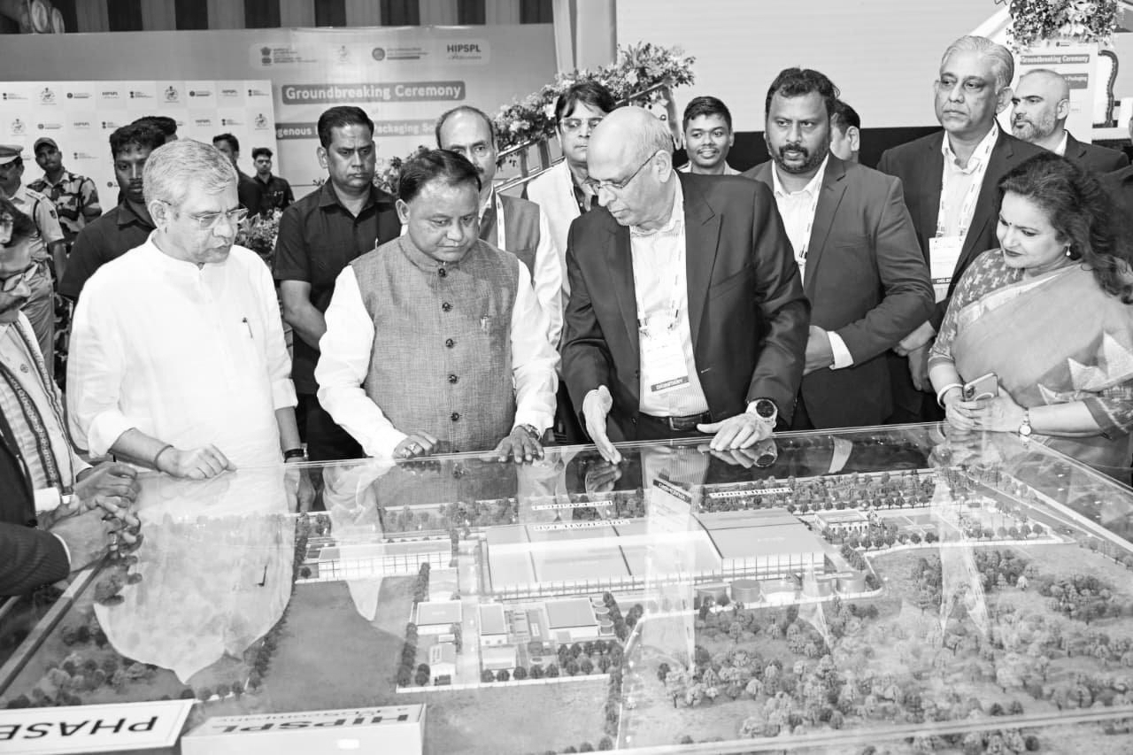
Odisha on Sunday took a major step into the global semiconductor supply chain as Chief Minister Mohan Charan Majhi and Union Minister Ashwini Vaishnaw laid the foundation stone for India’s first advanced 3D glass semiconductor packaging facility in Bhubaneswar.
The project is being developed by Heterogeneous Integration Packaging Solutions Pvt Ltd (HIPSPL) , a wholly owned Indian subsidiary of US-based 3D Glass Solutions Inc .
The plant, coming up at Info Valley in Bhubaneswar, has been approved with an investment of around Rs 1,943 crore and is expected to generate nearly 2,500 direct and indirect jobs .
Officials said the unit will manufacture advanced glass substrate semiconductor packaging products, including nearly 69,600 glass panel substrates annually, around 50 million assembled semiconductor units and more than 13,000 advanced 3D heterogeneous integration modules every year.
The “assembled units” refer to finished packaged semiconductor products rather than raw chips. These could include processors, AI accelerators, RF modules and defence electronics packages built using multiple semiconductor dies mounted on glass substrate panels.
Industry estimates suggest the broader global glass substrate semiconductor market currently runs into roughly 1.5 billion to 2 billion units annually , meaning the Odisha facility’s planned output of 50 million units a year will represent a meaningful early contribution in a highly specialised segment.
The project is expected to begin initial production over the next two to three years after construction and equipment installation are completed, with commercial ramp-up likely around 2028 . Full-scale capacity of 50 million assembled units annually is expected to be achieved gradually over the following years as customer orders and ecosystem support expand.