
NaMo Semiconductor Laboratory at IIT Bhubaneswar to boost India’s chip ecosystem
The Union Minister of Electronics and Information Technology, Shri Ashwini Vaishnaw, has approved the establishment of the NaMo Semiconductor Laboratory (Named after PM Modi) at the Indian Institute of Technology (IIT) Bhubaneswar. Funded under the Members of Parliament Local Area Development (MPLAD) Scheme, the project carries an estimated cost of ₹4.95 crore and aims to develop a strong talent pool for indigenous chip manufacturing and packaging across Bharat.
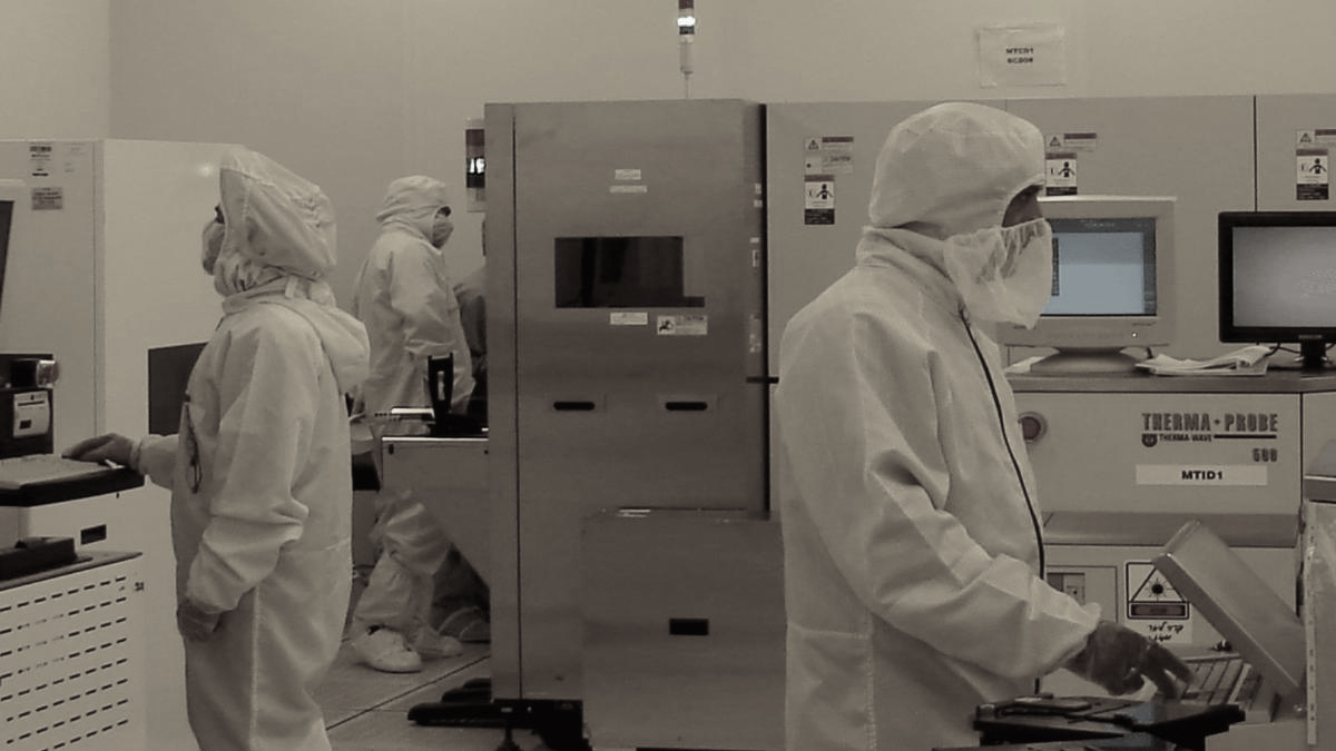
The lab is designed to equip students with industry-ready skills in semiconductor design, testing, and fabrication. It will provide access to state-of-the-art equipment, software, and cleanroom facilities, enabling hands-on experience with processes directly relevant to the chip industry. By bridging the gap between academic knowledge and industrial requirements, the lab ensures that graduates can seamlessly contribute to India’s rapidly growing semiconductor sector.
Beyond student training, the NaMo Semiconductor Lab will act as a research and development hub, supporting advanced projects in chip design, packaging, and fabrication. IIT Bhubaneswar, already home to the Silicon Carbide Research and Innovation Centre (SiCRIC), will leverage these facilities to foster innovation and support upcoming semiconductor manufacturing units across the country. SiCRIC focuses on research and development in Silicon Carbide (SiC) technology, providing a cleanroom environment and advanced facilities for high-power semiconductor applications. The lab will also facilitate the taping out of student-designed chips, integrating academic research into commercial chip development.
Strategic significance and national impact
Odisha has been selected for two semiconductor projects under the India Semiconductor Mission (ISM:
• SiCSem Pvt Ltd - India’s first commercial Silicon Carbide (SiC) compound semiconductor fabrication facility in Info Valley, Bhubaneswar, focusing on high-power applications like electric vehicles, renewable energy, and defense. Notably, SiCSem is a newly established company, less than two years old, yet it has been awarded one of the largest government-backed semiconductor projects in the country, a move that has raised eyebrows in the industry.
• 3D Glass Solutions Inc. (3DGS)- Advanced 3D glass packaging facility supported by global players, including Intel, enabling cutting-edge chip packaging and heterogeneous integration technologies.
These projects represent a total investment of over ₹4,000 crore and are expected to generate employment for thousands of skilled professionals, positioning Odisha as a key hub for semiconductor research and manufacturing. The NaMo Semiconductor Lab complements these initiatives by creating a pipeline of trained talent and fostering innovation, thereby strengthening India’s domestic semiconductor ecosystem and reducing dependence on imports.
Timeline and investment
The lab’s equipment and software have been budgeted at ₹4.6 crore and ₹35 lakh, respectively. While an official completion timeline has not been publicly announced, similar government-supported semiconductor projects typically become operational within 12–18 months, aligning with India’s push for rapid expansion in the sector.
With India already hosting 20% of the world’s chip design talent and students from 295 universities using advanced Electronic Design Automation (EDA) tools, the NaMo Semiconductor Laboratory is poised to become a catalyst for research, skilling, and industrial readiness, making IIT Bhubaneswar a strategic hub in the national semiconductor ecosystem.