
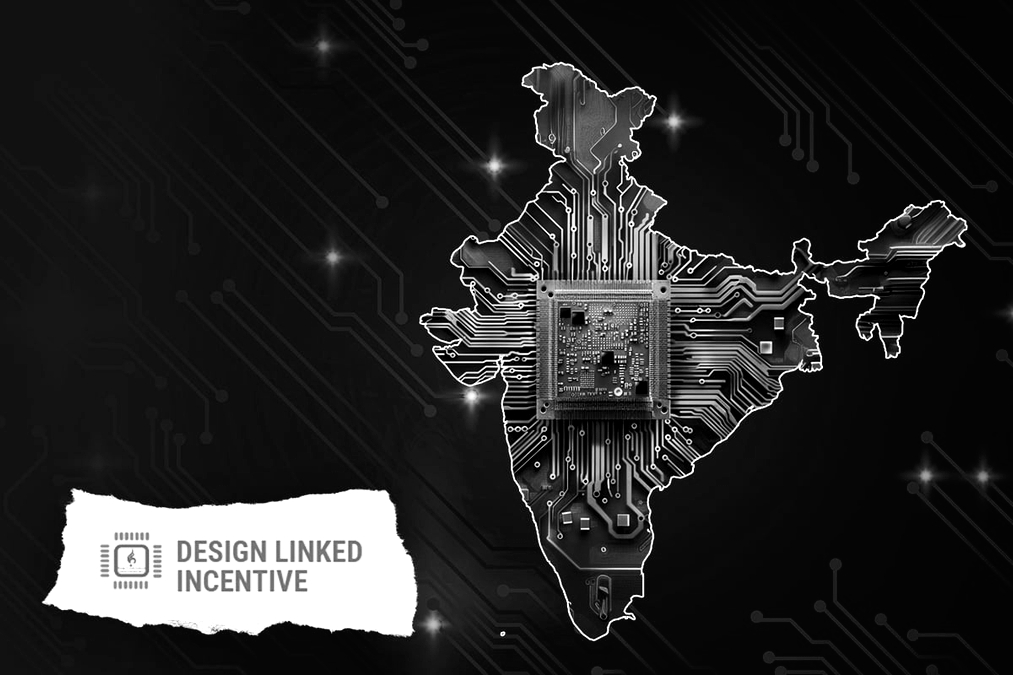
India’s semiconductor design projects show rapid growth under DLI scheme
India’s ambition to become a serious player in the global semiconductor value chain is steadily taking shape, with the Design Linked Incentive (DLI) Scheme emerging as a key pillar of this strategy. Announced under the Semicon India Programme and implemented by the Ministry of Electronics and Information Technology, the scheme focuses on strengthening India’s chip design ecosystem at a time when global supply chains remain vulnerable and heavily concentrated in a few countries.
Unlike semiconductor manufacturing, which demands massive capital investment, chip design is a high-value activity that relies on intellectual property, skilled talent, and innovation. Industry estimates suggest that design alone contributes up to half of a semiconductor’s total value. Recognising this, the government launched DLI in December 2021 with an allocation of around ₹1,000 crore to support domestic startups, MSMEs, and Indian-owned companies working on chip design.
So far, a modest but meaningful portion of this allocation has been sanctioned, largely in the form of reimbursements and sales-linked incentives tied to performance milestones. The spending model is deliberately phased, with funds released only when companies move from design to deployment, ensuring fiscal discipline while encouraging execution.
Under the DLI scheme, eligible startups and MSMEs can claim reimbursement of up to 50 per cent of their design and development costs, capped at ₹15 crore per project. Once a chip is successfully deployed in an electronic product, companies can also receive a deployment-linked incentive of 4 to 6 per cent on net sales for up to five years, capped at ₹30 crore. This makes DLI outcome-oriented rather than a blanket grant programme.
There has often been confusion around government assistance levels, particularly the mention of a 20 per cent subsidy. That figure applies to semiconductor fabrication and packaging units under the India Semiconductor Mission , not to the DLI scheme. DLI does not offer a flat capital subsidy. Instead, it supports design through cost reimbursements, access to advanced tools, and post-deployment incentives, reflecting the fundamentally different economics of chip design versus manufacturing.
Companies avail the scheme through a structured application process overseen by MeitY and implemented by C-DAC. Approved firms gain access to national-level design infrastructure through the ChipIN Centre, including high-end Electronic Design Automation tools, shared IP libraries, multi-project wafer prototyping, and post-silicon validation support. This shared infrastructure has significantly lowered entry barriers for Indian chip startups, which otherwise struggle with the high cost of global design tools.
The scheme has already supported 24 chip design projects across strategic areas such as surveillance systems, drone detection, energy meters, satellite communications, microprocessors, and IoT-based system-on-chips. More than 95 startups and companies are currently using the national EDA grid, while over 1,000 engineers have been engaged through DLI-supported projects.
In terms of geography, semiconductor design activity under DLI is largely concentrated in Karnataka , Tamil Nadu , Telangana , and Maharashtra , driven by their strong engineering talent base, startup ecosystems, and policy support. Bengaluru, Hyderabad, and Chennai have emerged as the primary design hubs, complementing manufacturing investments announced in Gujarat and Assam.
Several Indian companies have begun to stand out under the scheme. Vervesemi Microelectronics is developing motor-control chips for consumer appliances and electric mobility. InCore Semiconductors is working on indigenous RISC-V processor cores aimed at reducing India’s dependence on imported CPU IP. Netrasemi has taped out India’s first domestically designed AI-enabled surveillance chip at an advanced technology node, while Aheesa Digital Innovations is building indigenous broadband network chips using Indian processor architectures.
Globally, while Taiwan continues to dominate chip manufacturing, countries such as the United States , South Korea , and Japan lead in chip design and advanced IP creation. India’s DLI strategy mirrors this global reality by prioritising design first, allowing domestic firms to integrate into international supply chains even before large-scale fabrication becomes operational at home.
The DLI scheme is often compared with the Production Linked Incentive (PLI) framework. While both are performance-linked and outcome-driven, they serve different purposes. PLI rewards manufacturing output and scale, whereas DLI rewards innovation, design capability, and successful market deployment. Together, they form complementary pillars of India’s broader electronics and semiconductor strategy.
As India moves from policy intent to execution, the real test for DLI will be its ability to convert design success into sustainable products and global customers. Early indicators suggest the foundation is being laid carefully, focusing less on quick wins and more on building long-term technological depth.