
Bengaluru Firm Showcases AI-Powered Wafer Defect Detection at SEMICON India
Bengaluru-based deep-tech company RayVector Technologies is showcasing an AI-powered semiconductor inspection technology at SEMICON India 2026, demonstrating how advanced sensing, precision imaging and artificial intelligence can help manufacturers identify tiny wafer defects at an early stage and potentially prevent costly production losses.
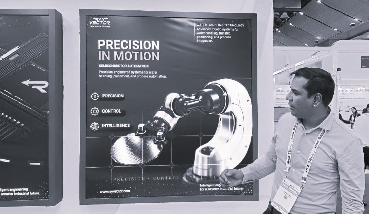
RayVector is demonstrating its multi-sensor module and wafer-handling technology at the event, being held at Yashobhoomi in Dwarka from September 17 to 19. According to the company, its system combines sensing, high-precision imaging and AI-based analysis to detect minute irregularities on semiconductor wafers within seconds. The company says its technology is being used by global semiconductor companies including Samsung, Intel and TSMC.
The demonstration comes as semiconductor manufacturing increasingly relies on AI, computer vision, precision imaging and intelligent sensing alongside conventional fabrication processes. RayVector said its work spans research, design, engineering, product development and scaling, with applications in semiconductor inspection, automated analysis and AI-enabled manufacturing. Its approach also incorporates physics-based engineering and synthetic data to support AI model development for specialised semiconductor applications.
Wafer inspection is crucial because semiconductor production involves multiple highly precise stages, and even tiny defects can affect chip quality and manufacturing yields. AI-assisted inspection can analyse large volumes of imaging and sensor data to identify anomalies early, helping manufacturers investigate process issues before defective material advances through additional production stages.
RayVector Founder and CEO Shrikant K. Avadhani said the company aims to convert complex semiconductor research into commercial products. He said RayVector is increasingly focusing on proprietary sensor and vision technologies to develop globally relevant semiconductor products from India.
CTO Chakravarthy Elumalai said the company is focused on taking innovation beyond the laboratory and turning it into practical and scalable products.
RayVector operates in India and the US, with an engineering presence in Tualatin, Oregon. The company says its Indian R&D capabilities and engagement with the US semiconductor ecosystem are supporting its international expansion.
The development comes as India broadens its semiconductor ambitions beyond fabs. Semicon 2.0, approved in July 2026 with an outlay of ₹1,27,500 crore, covers chip design, machines and materials, fabs, advanced packaging, R&D and talent development. The government says 12 semiconductor projects worth more than ₹1.64 lakh crore have been approved, while 24 chip-design projects worth about ₹900 crore have also received approval.
With more than 500 exhibitors from over 20 countries, SEMICON India 2026 underscores India's effort to build a wider semiconductor ecosystem. RayVector's demonstration highlights the growing role of AI-powered inspection, indigenous equipment technology and semiconductor intellectual property in that expansion.